- 您现在的位置:买卖IC网 > Sheet目录2000 > IDT5V41064NLGI (IDT, Integrated Device Technology Inc)IC CLK GEN 1:1 16QFN
IDT5V41064
1 OUTPUT PCIE GEN1/2 SYNTHESIZER
IDT 1 OUTPUT PCIE GEN1/2 SYNTHESIZER
8
IDT5V41064
REV G 112111
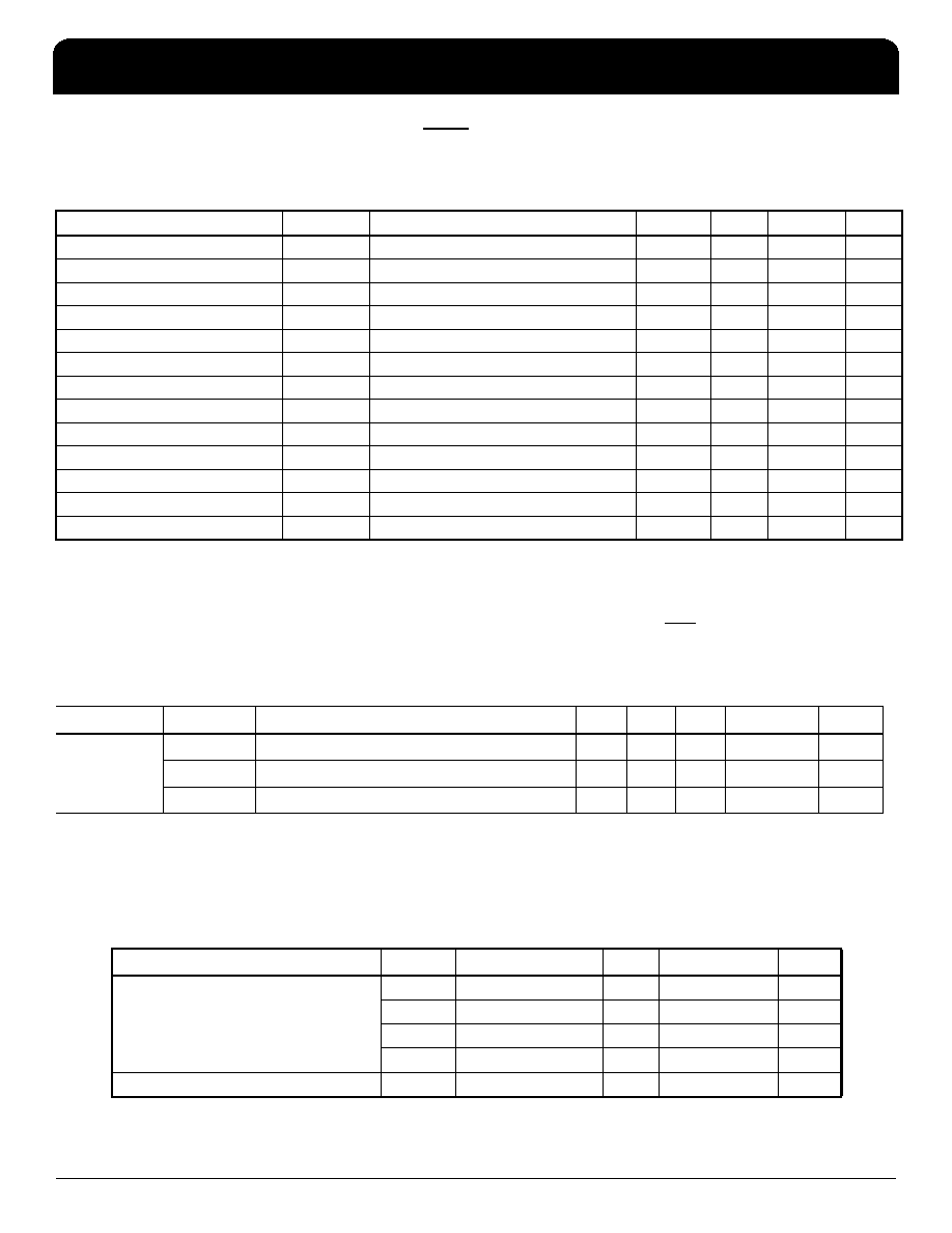
AC Electrical Characteristics - CLK/CLK
Unless stated otherwise, VDD=3.3 V ±5%, Ambient Temperature -40 to +85
° C
1 Test setup is R
S=33 ohms RP=50 ohms with 2 pF, RR = 475Ω (1%).
2 Measurement taken from a single-ended waveform.
3 Measurement taken from a differential waveform.
4 Measured at the crossing point where instantaneous voltages of both CLK and CLK are equal.
Electrical Characteristics - Differential Phase Jitter
Note 1. Guaranteed by design and characterization, not 100% tested in production.
Note 2. See http://www.pcisig.com for complete specs.
Note 3: Applies to 100MHz, spread off and 0.5% down spread only.
Thermal Characteristics
Parameter
Symbol
Conditions
Min.
Typ.
Max.
Units
Input Frequency
25
MHz
Output Frequency
100
MHz
Output High Voltage1,2
VOH
660
700
850
mV
Output Low Voltage1,2
VOL
-150
0
27
mV
Crossing Point Voltage1,2
Absolute
250
350
550
mV
Crossing Point Voltage1,2,4
Variation over all edges
40
140
mV
Jitter, Cycle-to-Cycle1,3
25
100
ps
Rise Time1,2
tOR
From 0.175 V to 0.525 V
175
332
700
ps
Fall Time1,2
tOF
From 0.525 V to 0.175 V
175
344
700
ps
Rise/Fall Time Variation1,2
75
125
ps
Duty Cycle1,3
45
51
55
%
Stabilization Time
tSTABLE
From power-up VDD=3.3 V
1.2
3.0
ms
Spread Change Time
tSPREAD
Settling period after spread change
3.0
ms
Parameter
Symbol
Conditions
Min
Typ
Max
Units
Notes
Jitter, Phase
tjphasePLL
PCIe Gen1
30
86
ps (p-p)
1,2,3
tjphaseLO
PCIe Gen2, 10 kHz < f < 1.5 MHz
1.2
3
ps (RMS)
1,2,3
tjphaseHIGH PCIe Gen2, 1.5 MHz < f < Nyquist (50 MHz)
1.9
3.1
ps (RMS)
1,2,3
Parameter
Symbol
Conditions
Min.
Typ.
Max.
Units
Thermal Resistance Junction to
Ambient
θJA
Still air
63.2
° C/W
θJA
1 m/s air flow
55.9
° C/W
θJA
2 m/s air flow
53.1
° C/W
θJA
3 m/s air flow
51.4
° C/W
Thermal Resistance Junction to Case
θJC
65.8
° C/W
发布紧急采购,3分钟左右您将得到回复。
相关PDF资料
IDT5V41066PGG
IC CLK GEN SPRED SPECTRM 20TSSOP
IDT5V49EE901NLGI8
IC PLL CLK GEN 200MHZ 32VFQFN
IDT5V49EE902NLGI
IC CLOCK GEN PLL 500MHZ 32VFQFPN
IDT5V49EE904NLGI8
IC PLL CLK GEN 200MHZ 32VFQFN
IDT821024PPG
IC PCM CODEC QUAD NONPROG 44TQFP
IDT821034DNG
IC PCM CODEC QUAD MPI 52-PQFP
IDT821054PQF
IC PCM CODEC QUAD MPI 64-PQFP
IDT82V3001APVG8
IC PLL WAN W/SGL REF INP 56-SSOP
相关代理商/技术参数
IDT5V41064NLGI8
制造商:Integrated Device Technology Inc 功能描述:IC CLOCK BUFFER ZD 2.5V 16QFN
IDT5V41065NLG
制造商:Integrated Device Technology Inc 功能描述:IC CLK GEN SPRED SPECTRM 16NLG
IDT5V41065NLG8
制造商:Integrated Device Technology Inc 功能描述:IC CLK GEN SPRED SPECTRM 16NLG
IDT5V41065NLGI
制造商:Integrated Device Technology Inc 功能描述:IC CLK GEN SPRED SPECTRM 16NLG
IDT5V41065PGG
功能描述:IC CLK GEN SPRED SPECTRM 16TSSOP RoHS:是 类别:集成电路 (IC) >> 时钟/计时 - 专用 系列:PCI Express® (PCIe) 标准包装:1,500 系列:- 类型:时钟缓冲器/驱动器 PLL:是 主要目的:- 输入:- 输出:- 电路数:- 比率 - 输入:输出:- 差分 - 输入:输出:- 频率 - 最大:- 电源电压:3.3V 工作温度:0°C ~ 70°C 安装类型:表面贴装 封装/外壳:28-SSOP(0.209",5.30mm 宽) 供应商设备封装:28-SSOP 包装:带卷 (TR) 其它名称:93786AFT
IDT5V41065PGG8
制造商:Integrated Device Technology Inc 功能描述:IC CLK GEN SPRED SPECTRM 16TSSOP
IDT5V41065PGGI
功能描述:IC CLOCK SYNTHESIZER 16TSSOP RoHS:是 类别:集成电路 (IC) >> 时钟/计时 - 专用 系列:- 标准包装:1 系列:- 类型:时钟/频率发生器,多路复用器 PLL:是 主要目的:存储器,RDRAM 输入:晶体 输出:LVCMOS 电路数:1 比率 - 输入:输出:1:2 差分 - 输入:输出:无/是 频率 - 最大:400MHz 电源电压:3 V ~ 3.6 V 工作温度:0°C ~ 85°C 安装类型:表面贴装 封装/外壳:16-TSSOP(0.173",4.40mm 宽) 供应商设备封装:16-TSSOP 包装:Digi-Reel® 其它名称:296-6719-6
IDT5V41065PGGI8
制造商:Integrated Device Technology Inc 功能描述:IC CLK GEN SPRED SPECTRM 16TSSOP